
Key Takeaways
- Chip silicon starts as sand, purified to less than one foreign atom per billion, then grown into a 300 mm crystal sliced into wafers.
- Circuits are printed with light: EUV machines vaporise tin droplets 50,000 times a second to make 13.5 nm light, a technology unique to ASML.
- A "3 nm" chip contains nothing that measures 3 nm — Intel admits node names no longer refer to any specific measurement.
It starts as sand and ends as the most precise manufacturing humans do
Silicon is the second most abundant element in the Earth's crust, and sand is full of it. What separates beach sand from the chip in your phone is not the material — it is purity and precision at scales that defy intuition. Silicon earns the job because it is a semiconductor: as Intel puts it, it can be turned into an excellent conductor or an insulator of electricity with minor amounts of impurities added. Everything in computing is built on that switchable personality.
From sand to a flawless crystal
The raw silicon is purified to a standard Intel states as less than one alien atom per billion, then melted and cooled into a solid crystal cylinder called an ingot — 300 millimetres across and weighing about 100 kilograms. The ingot is sliced into wafers about one millimetre thick, each polished to a flawless, mirror-smooth surface, because the circuits about to be printed on it are thousands of times smaller than a dust speck. Hundreds of chips are built on a single wafer before it is tested, diced and packaged.
Printing circuits with light
The printing process is photolithography, and it works like photography crossed with a stencil. A light-sensitive material called photoresist coats the wafer. Ultraviolet light shines through a mask — a stencil carrying one layer's circuit pattern — and through a lens that shrinks the pattern onto the wafer. A chemical process then washes away the exposed or unexposed resist, leaving the pattern behind. Repeat, layer upon layer: today's chips may stack more than 30 layers of circuitry, where Intel's 1971 4004 had five.
The frontier version of this printing uses extreme ultraviolet light, and only one company on Earth makes the machines. ASML's EUV technology uses light with a wavelength of 13.5 nanometres — more than 14 times shorter than the 193-nanometre light of the previous generation. Making that light is a small controlled explosion, repeated relentlessly: molten tin droplets about 25 microns wide are fired at 70 metres per second, a first laser pulse flattens each droplet into a pancake, and a second, more powerful pulse vaporises it into a plasma that glows in EUV. This happens 50,000 times every second to produce enough light to manufacture chips.
Doping: the deliberate impurity that makes it a switch
Between printing steps comes the move that creates electronics. Ions — charged atoms — are embedded beneath the wafer's surface in the regions the photoresist leaves uncovered, a process called ion implantation. In Intel's description, this alters the conductive properties of the silicon in selected locations, leaving certain regions "doped with alien atoms." Regions doped one way conduct differently from regions doped the other way, and where they meet, you get a transistor.
A transistor is, at heart, a switch with no moving parts. Intel's own summary: transistors "act as switches, either preventing or allowing electrical current to pass through," and a gate turns them on and off, letting currents "send, receive, and process digital data (1s and 0s)." A modern chip interconnects billions of these switches with metal wiring Intel compares to a multi-level highway.
Moore's law, and the lie in the node names
In 1965 Gordon Moore predicted the number of transistors on a chip would double every year; in 1975 he revised it to roughly every couple of years. Intel's stated position, in its CEO's words, is that "Moore's Law is alive and well" — sustained in recent decades as much by new transistor architectures as by raw shrinkage.
But the generation labels have quietly detached from reality, and Intel has admitted it in writing. Its 2021 process fact sheet states that today's node names "no longer refer to any specific measurement," and that "Intel's node numbers do not represent the actual dimension of any physical feature on a transistor." That is why Intel renamed its own roadmap — Intel 7 (formerly its 10-nanometre process), Intel 4 (formerly 7-nanometre), then Intel 20A, invoking the angstrom era. When any maker sells you a "3 nm" or "2 nm" chip, the number is a generation name — a rough claim about density and performance — not the size of anything you could measure on the die.
The Twikup Take
A chip is sand that has been purified past one stray atom in a billion, printed with light made by vaporising tin fifty thousand times a second, and deliberately contaminated in patterns a thousand times finer than a hair — so that billions of switches can pretend to be a mind. The industry's marketing numbers have drifted free of the physics, but the physics itself keeps delivering: the most complex objects humans manufacture in bulk begin as the stuff on a beach.
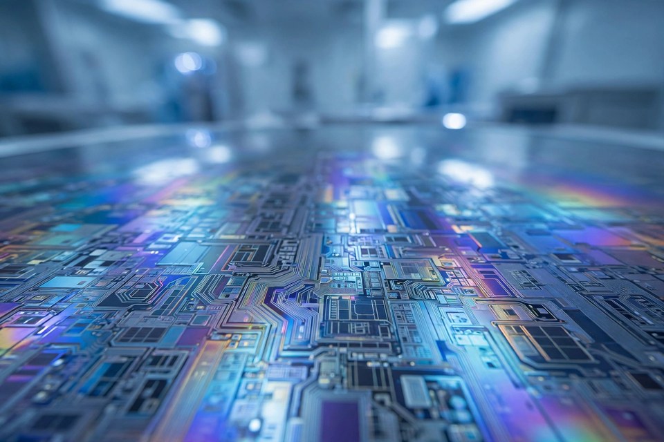
Image: Illustrative image.